State Variable Filters: Three Outputs, Independent Tuning and Notch Design
- Published
- Author
- Komal Ganvir
- Reads
- 347
A state variable filter derives low-pass, high-pass and band-pass responses from one op-amp circuit, with a fourth notch output available by adding a summing stage.
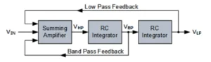
A state variable filter is useful when a design needs several second-order responses from one active RC circuit. Two op-amp integrators and a summing amplifier produce low-pass, high-pass and band-pass outputs; another summing stage can add a notch response. In a properly designed circuit, the centre frequency and quality factor, Q, can be adjusted independently, which makes this topology practical for tunable signal paths.
How the three outputs form
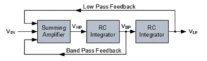
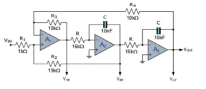
The summing amplifier combines the input with feedback from the integrator stages. Its output is the high-pass response, VHP. The first integrator processes that signal to produce the band-pass response, VBP, and the second integrates VBP to produce the low-pass response, VLP. The circuit’s feedback connections set how these stages interact and shape the response.
This arrangement makes all three responses available at different points in the same circuit. A low-pass output attenuates frequencies above its operating region; a high-pass output attenuates those below it. The band-pass output selects a frequency range around the centre frequency, with its bandwidth determining how broad that range is.
Integrator and summing stages
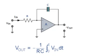
Each integrator uses a capacitor in the op-amp feedback path. For an ideal inverting integrator, the transfer function is:
Vout/Vin = -1/(sRC)
Here, R is the input resistance, C is the feedback capacitance, and s is the complex frequency variable. The minus sign indicates that the output is inverted. Cascading two such stages supplies the band-pass and low-pass responses, while the summing amplifier closes the feedback loop and generates the high-pass output.
The summing amplifier acts as an adder-subtractor. Its resistor network sets how the input, VBP and VLP contribute to the signal that drives the integrators. Those feedback proportions affect damping and the overall frequency response, so component values for this stage depend on the chosen circuit topology.
Setting centre frequency and Q
With identical integrator resistors and capacitors, the natural frequency is:
f0 = 1/(2πRC)
Changing either R or C shifts the frequency. In a suitable design, that adjustment can leave Q substantially unchanged. This separation is useful when tuning a filter: the selected centre frequency need not dictate the response’s selectivity.
Q describes the sharpness of the band-pass response. For that response, Q = f0/BW, where BW is the difference between the upper and lower -3 dB frequencies. A higher Q gives a narrower bandwidth and sharper peak; a lower Q gives a wider passband. For a standard second-order response, the damping ratio is ζ = 1/(2Q), so higher Q corresponds to lower damping.
Example: a 1 kHz filter
For a target natural frequency of 1 kHz, Q of 10, and equal R and C values in both integrators, choosing 10 nF capacitors gives:
R = 1/(2πf0C)
R = 1/(2 × π × 1000 × 10 × 10-9) ≈ 15.9 kΩ
The resulting integrator values are C = 10 nF and R ≈ 15.9 kΩ, or approximately 16 kΩ. These values set the natural frequency for the stated equal-component arrangement. The other resistor values must be worked out from the specific summing-amplifier topology and its equations; the information here does not supply enough detail to calculate them or verify the complete gain.
Adding and tuning a notch output
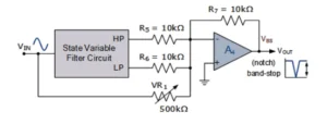
A notch, or band-stop, response can be formed by adding an op-amp summing stage that combines VLP and VHP. Their combined response produces a rejection around the band-pass centre frequency, while frequencies outside that region pass through. The notch frequency therefore corresponds to the centre frequency of the band-pass response.
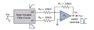
Notch depth depends on the signals and resistor network used by the added stage. Including VBP or the original input, VIN, provides further control over the resulting shape. Q sets the notch bandwidth and selectivity; it does not, by itself, set the notch depth.
Where the topology fits
One circuit can supply three filter responses, and an extra summing amplifier extends it to a notch. Together with the ability to tune centre frequency and Q independently in an appropriate design, that makes the state variable topology a useful choice for adjustable filtering. Applications include audio signal processing, frequency selection, communication systems, electronic instrumentation, active filters and signal conditioning.
For design work, the key distinction is between frequency setting and response shaping: the integrator R and C values establish the natural frequency, while the feedback and summing network determine damping, Q and the form of the outputs. The notch stage adds another design choice, with its resistor ratios governing rejection depth.