Near-Threshold Edge AI SoCs: Where Foundation IP Meets the Power Wall
- Published
- Author
- Andrew Appleby
- Reads
- 417
Near-threshold operation at 0.4–0.5V can cut edge AI SoC power, but memory, logic and I/O IP must be characterized and validated early to keep timing predictable.
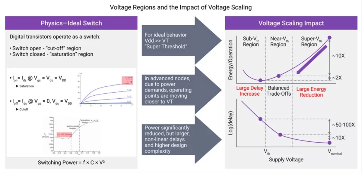
Voltage scaling used to be the easy lever for SoC power. In advanced FinFET processes, going much below roughly 0.4–0.5V turns that lever into a design risk. That's the tension edge AI chips now face. They have to run inference close to the sensor or endpoint while staying inside tight energy and thermal budgets. The payoff from near-threshold operation is large, but the chip stops behaving the way nominal-voltage models predict.
Why near-threshold changes the rules
Lowering the supply still cuts energy per operation. The trouble is what else moves with it. As Figure 1 shows, delay climbs steeply, variability grows and noise margins shrink.
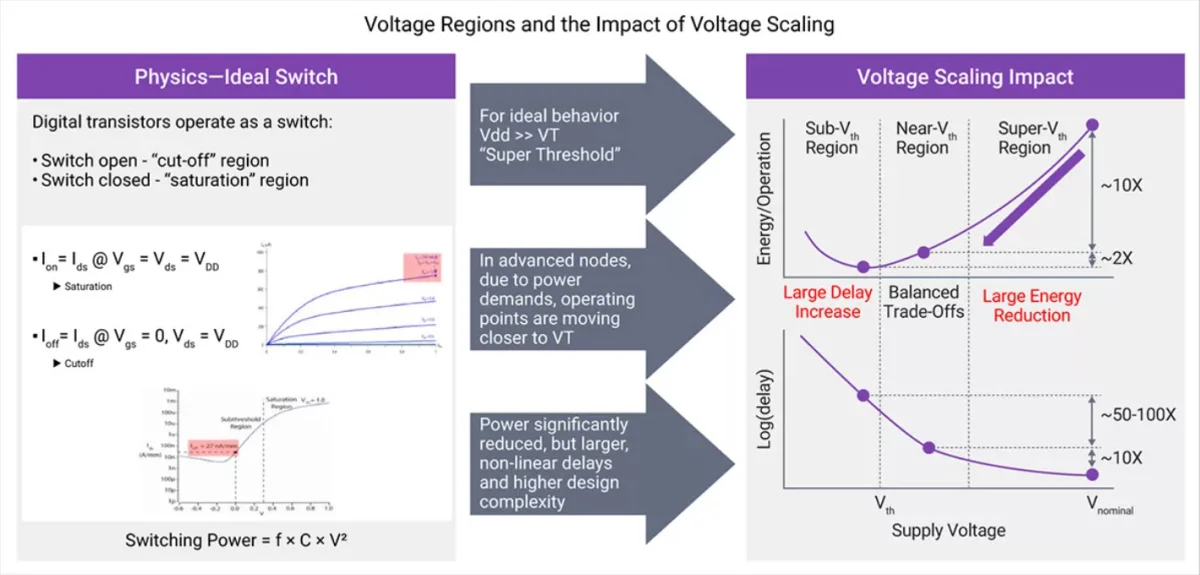
Fig. 1: Energy efficiency improves at lower voltage, but delay and variability increase sharply near threshold.
In practice, that shows up in four ways:
- Timing paths react strongly to small voltage variations
- IR drop and local droop become first-order effects rather than corrections
- Guard-banding loses effectiveness
- Nominal-voltage models stop predicting silicon behavior with useful accuracy
Here's the thing: voltage stops being a single knob. It couples timing, power integrity, memory behavior and signoff, so a change in one place ripples through the whole stack.
Memory usually sets the voltage floor
Embedded memory takes a large share of area and power, and if it isn't architecturally decoupled from logic, it often determines the minimum operating voltage (Vmin). Synopsys describes two routes that its Foundation IP addresses:
- Single-rail memories with silicon-validated assist features, supporting operation down to ~600 mV Vmin. That gives a direct V² energy reduction without restructuring the architecture.
- Dual-rail memories that separate logic and memory supplies, so compute blocks can scale further. Synopsys reports this approach was validated at ISSCC 2025 with a 38 Mb/mm² dual-rail SRAM operating at 380/540 mV in 3nm FinFET.
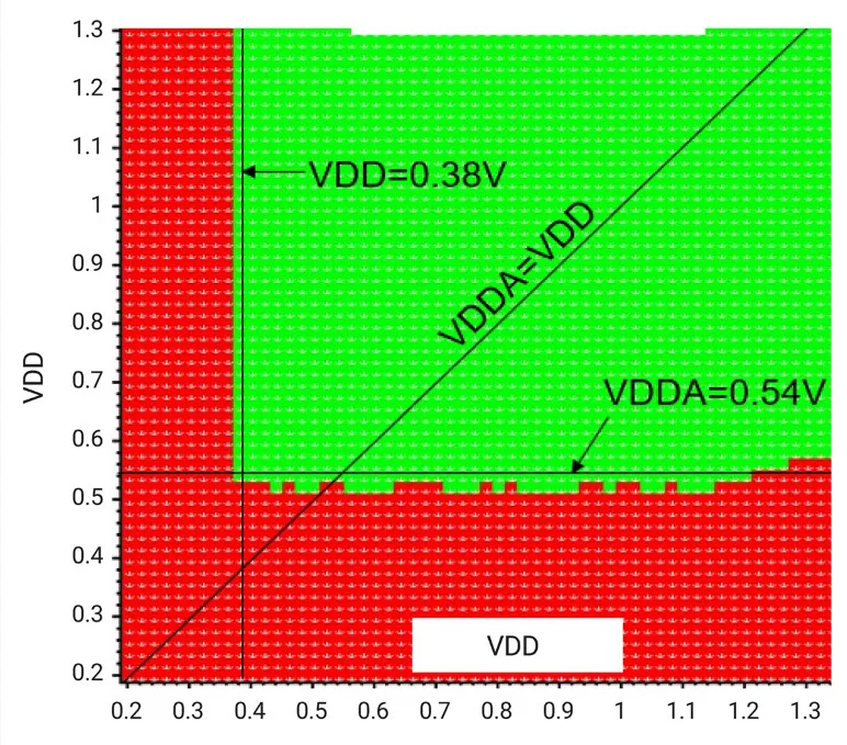
Fig. 2: Dual-rail memory architecture decouples logic and memory VDD, validated at ISSCC 2025 with a 38 Mb/mm² SRAM at 380/540 mV in 3nm FinFET.
Ultra-low-power register files round out the set for localized storage in compute-heavy regions. The right choice depends on the block. MAC tiles tend to suit small, distributed SRAM blocks, activation units benefit from ULP register files with wide data paths, and shared system buffers usually need high-bandwidth AXI interfaces.
Logic libraries and I/O: the less glamorous limits
Logic libraries built for low voltage need more than a re-run of the nominal characterization. Synopsys points to several areas of emphasis: moment-based LVF timing and noise models across wide PVT coverage, delay and slew models that capture near-threshold non-linearity, and expanded verification for MIS effects, pulse-width integrity, skew interactions and mixed-device behavior. It also cites targeted silicon validation with extended timing and functional sweeps to confirm model accuracy. Without that accuracy, the surprises tend to show up at low-voltage signoff or on silicon.
I/O is the other ceiling. In many designs the I/O domains set system-level Vmin, so a well-optimized core gains little if the periphery can't follow it down. Synopsys lists a portfolio that covers control interfaces (GPIO, I3C/I2C, SWI3S), high-speed links (LVDS, RGMII), clock and reference inputs, storage (SD/eMMC), test I/O, and 2.5D/3D integration I/O for chiplet-based systems. The company says each is validated for consistent operation across supply levels.
Closing the loop between IP, tools and silicon
Predictable operation at roughly 0.4–0.5V depends on alignment across IP, EDA flows, modeling and silicon. Synopsys frames this as an iterative, closed-loop process, shown in Figure 3:
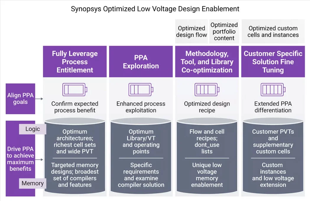
Fig. 3: A closed-loop methodology aligns Foundation IP, tools, and silicon feedback to ensure optimized low-voltage design.
- Early exploration of PPA trade-offs against specific voltage targets
- Choice of IP architecture, technology options and configuration, with cell tuning where needed
- Flow and signoff refinement for low-voltage conditions
- Silicon feedback that tightens model accuracy over time
Synopsys says its application engineers sit between IP and EDA developers and SoC design teams during customer engagements, so the features get used properly and the technology is deployed where it fits best.
A ~20% power cut, reported by Synopsys
Synopsys describes a power-sensitive AI networking SoC targeting high volumes in an advanced node. The design used near-threshold operation at extremely low voltages and ran on a very compressed schedule. The IP package included specially tuned low-voltage logic cells, custom level shifters, a custom dual-rail memory compiler, and a targeted PVT corner set chosen for the best power efficiency through near-threshold signoff.
The reported results were:
- ~20% reduction in power consumption
- Performance and area targets fully met
- No schedule impact
- Lower validation complexity and no re-spins
These are vendor-reported outcomes from a single design, so treat them as a data point rather than a benchmark. The more useful signal is the pattern: custom cells, level shifters and memory compilers were tuned together rather than bolted on after the core was built.
Where this goes next
Synopsys positions its support as more than IP delivery. It cites documentation, design reviews, PPA tuning sessions, DTCO and PPA exploration to help customers choose configurations, and custom characterization for specialized requirements. The company also argues that a broad IP portfolio with consistent design across wide voltage ranges eases reuse across process generations and foundries.
My read is that the real decision is timing. Settling voltage targets, IP configurations and low-voltage methodology after RTL is frozen is where schedules slip. The power wall is real, but teams that engage early on memory architecture and I/O voltage limits have a far better shot at getting through it. Synopsys's white paper, Beating the Edge AI Power Wall with Low Voltage Foundation IP, goes deeper on the methodology.