AI Agents Could Expand Semiconductor Engineering Without Replacing Verified EDA Tools
- Published
- Author
- Jim Shiely
- Reads
- 759
AI can cut the effort behind engineering experiments and coordinate EDA workflows, while models, metrology and verification keep decisions grounded in evidence.
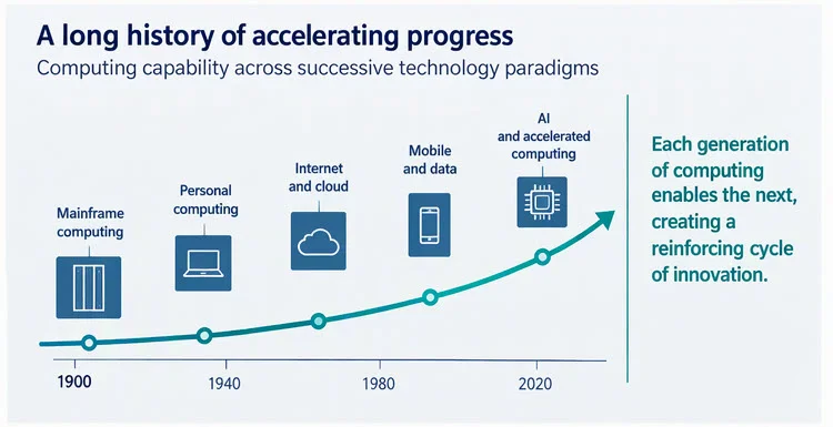
AI is starting to change the pace of semiconductor engineering by reducing the work needed to build software, operate engineering tools and run analyses. The practical shift is not simply that engineers can ask a model for an answer. Generative AI can make experiments cheaper to set up, while agentic systems can coordinate longer workflows. The results still depend on qualified models, physical measurements and deterministic verification.
This creates a feedback loop: better computing supports better design and manufacturing tools, which help produce the next generation of computing hardware. Ray Kurzweil described a broader version of this pattern as the Law of Accelerating Returns. In a white paper on AI and IC innovation, Siemens applies that idea to semiconductor engineering. Across successive computing paradigms, accumulated tools, knowledge and capacity help engineers create what comes next.
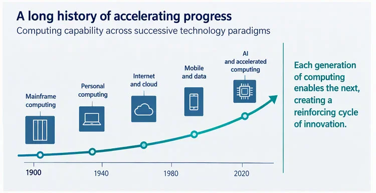
Fig. 1: Each computing generation contributes tools and capacity that help create the next.
More experiments for the same engineering effort
Semiconductor progress doesn’t trace a smooth exponential curve. It tends to move when a bottleneck becomes manageable enough for engineers to attempt work that once demanded too much time, money, computation or coordination.
Machine learning in computational lithography offers an example. Early demonstrations showed promise, but production use depended on several pieces maturing together: developers with both machine learning and semiconductor expertise, representative data, model management, intellectual property controls and customer confidence. A capable model alone wasn’t enough.
Generative AI targets a different source of friction: the effort required to work through complex EDA flows and build prototypes. Developing an original SPIE machine-learning course for lithography took roughly 200 to 300 hours, including some assistance with training data. In a later experiment, generative AI helped recreate and extend much of that prototype functionality in roughly 30 hours.
Those were notebook-level prototypes, not production computational-lithography tools. The comparison therefore says something about exploratory effort, not production readiness or equivalent results. Still, reducing setup time can let experienced silicon engineers examine more alternatives within the same schedule, with less effort spent on software mechanics.
Agents coordinate work; engineering tools establish authority
Agentic AI extends assistance from producing an analysis or prediction to coordinating sequences of work. A language model can interpret an engineer’s intent, gather relevant context, assemble a workflow and call specialized tools. The analysis and its engineering authority remain with the EDA tools, qualified models, validated data and deterministic checks.
That division matters because semiconductor workflows rely on expert judgment: which analysis to run, what data applies, whether a result is credible and when an exception needs closer review. Expertise takes years to build, while computational capacity and demand can grow much faster.
In computational lithography, for example, an agent could gather recent scanning electron microscope (SEM) measurements, configure model calibration, run an analysis, inspect convergence and runtime, then return exceptions to an engineer. The aim is to let each specialist direct more computation and tool activity, while retaining human judgment where interpretation matters.
Siemens Fuse EDA AI follows this architecture by connecting AI models with EDA tools, engineering knowledge, specialized languages and data formats.
Metrology ties computation to silicon
Computational lithography shows why physical evidence remains central. A fab collects wafer and metrology data, calibrates models, uses them to guide corrections, measures the resulting silicon and feeds those observations into later calibration and process changes. Repeated comparison with manufactured results helps establish where a model can be relied upon.
The loop uses several kinds of computation, each with a different job. Physics-based simulation predicts physical behavior. Qualified models, rule decks and deterministic verification provide engineering checks and signoff authority. Specialized machine learning supports prediction, classification and optimization. Generative AI can make knowledge and tools easier to access; agents can coordinate workflows; accelerated computing can fit more analyses into practical schedules.
Together, these methods turn physical understanding and manufacturing observations into interventions that engineers can assess. Simulation guides exploration, metrology records what happened, models compare prediction with observation, and engineering changes alter the design or process.
As EDA tools, manufacturing systems and digital twins become accessible to agents, coordination can extend across more of this loop. Agents could explore design and technology tradeoffs, run simulation and computational-metrology flows, compare alternatives and organize evidence for an engineer’s next decision.
Trust becomes part of the workflow
Faster analysis raises the value of trustworthy inputs and results. AI can produce hypotheses, assemble workflows and explore alternatives quickly. Engineers still need evidence they can act on: verified designs, qualified models, measured silicon and data with understood origins and applicability.
That calls for engineering context, controlled data access, traceable actions, deterministic checks and human control over consequential decisions. These are working parts of an agentic EDA system, not extras to add after a workflow has been built.
A Calibre nmOPC model, for instance, earns confidence through calibration against physical metrology and continued comparison with wafer results. The model, calibration data, process conditions and physical measurements together define where its predictions are useful. When conditions change, recalibration can extend the evidence base. AI-enhanced metrology tools such as Canopus can contribute by increasing the quantity and quality of SEM data available for calibration.
Calibre, along with foundry-qualified rule decks and verification flows, checks whether a design meets manufacturing requirements. Agents can coordinate more analyses and explore more options, while trusted engineering tools determine which results satisfy the required checks.
As tools become easier to use, constraints elsewhere in the organization can take up more of the cycle. Establishing data access, protecting intellectual property and authorizing production changes may limit the pace of work. The time needed to put access, protection and decision authority in place becomes another engineering problem to solve.
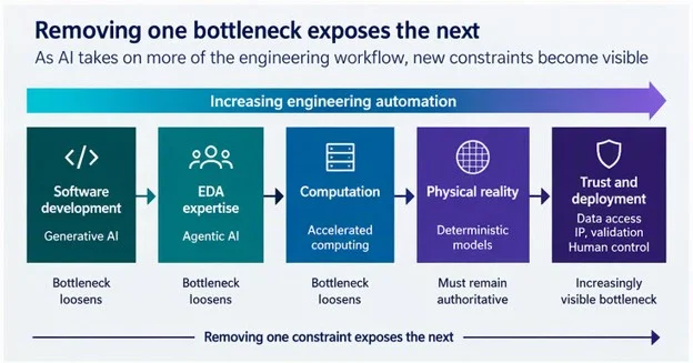
Fig. 2: When analysis speeds up, evidence, verification, data access, intellectual property protection, validation and human control make up more of the remaining cycle.
An engineering loop that keeps changing
Better hardware expands AI capability; AI lets engineers explore and automate more work; manufacturing supplies physical evidence; and verification establishes which results can proceed. Each improvement shifts the bottleneck.
The useful measure of this acceleration is therefore not how quickly an agent can produce an answer. It is whether engineers can move through more of the loop while preserving the evidence and checks needed to trust the result. The next gains will depend on identifying the constraint that now limits the work, then using measured silicon and qualified tools to guide the next design and process decisions.